- How to use “real” UART
- Arduino’s Automatic Reset
- Linux always toggles DTR & RTS
- Espressif’s Automatic Reset
- Talking to Espressif’s Bootloader
- The ESP32-S2 reset pin
- Reproducing Espressif’s reset circuit
- The missing part of Espressif’s reset circuit
- Transistors in reverse and redundant circuits
- The serial TX path seems to be down
I recently discussed how Espressif implements automatic reset, a feature that lets users easily update the code on an Espressif microcontroller. There are actually more subtleties than a quick look would suggest, and I spent a fair bit of time investigating them. This article and the next two present (The missing part of Espressif’s reset circuit and Overanalyzing a minor quirk of Espressif’s reset circuit) what I have learned.
The current article simply focuses on reproducing that circuit with basic components, both to make sure we understand what it is made of, and to be able to play with it more easily.
A small reminder
We’ll be using the ESP-Prog, which is a combined UART and JTAG USB adapter. It implements the same reset circuit as the Espressif development boards, but we can more easily peek at EN and IO0.

If we download the reference documents for the ESP-Prog and open the schematics, we can find the logic circuit that connects DTR and RTS from UART to EN and IO0 on the microcontroller. This same diagram is shown in the “Automatic Download Function” section of the online documentation.

It is actually easy to find the circuit on the board; look for a pair of components labelled “J3Y” next to the FT2232HL chip:

As discussed before, this circuit sets the electrical level of EN and IO0 to high/low depending on the electrical levels of DTR and RTS. Specifically:
| Asserted | DTR | RTS | EN | IO0 | Function |
|---|---|---|---|---|---|
| Neither | 3.3 V | 3.3 V | 3.3 V | 3.3 V | Normal run |
| RTS & DTR | 0 V | 0 V | 3.3 V | 3.3 V | Normal run |
| RTS | 3.3 V | 0 V | 0 V | 3.3 V | Off |
| DTR | 0 V | 3.3 V | 3.3 V | 0 V | Bootloader |
The purpose of this circuit is to be able to reset the chip, either normally or into bootloader mode, using the UART control lines (DTR and RTS). And all this without resetting the chip when opening the serial device (to send and receive data). Indeed, opening the serial device automatically brings DTR and RTS to a low electrical level, and this is unavoidable on Linux. A naive use of e.g. toggling RTS to reset would trigger unwanted resets.
This means that 2 out of the 4 input DTR/RTS combinations need to behave the same. Thus, only 3 states exist. As a result, one output EN/IO0 combination cannot be reached. Indeed, with this circuit, you cannot put both EN and IO0 to a low electrical state at the same time. However, this does not matter since the chip is off in this situation.
Probing the ESP-Prog
To observe this, I used my Rigol DS1054, which is a 4-channel oscilloscope. This allowed me to observe simultaneously DTR, RTS, EN and IO0.
First, to observe DTR and RTS before the logic circuit, I used some IC clamps (9 € on AliExpress) to tap directly to the pins of the FT2232HL chip. In the documentation of the ESP-Prog, we can see which pins are used for what:

Thus, we tap into the pins 40 and 43 of the chip:


To measure the outputs EN and IO0, I simply use wires with female Dupont connectors on the “Program” (UART) port of the ESP-Prog. I also need a couple of wires for ground (I can connect the ground of two probes using the same wire).

COM1 and JTAG as COM2 (on Windows). On Linux, this will be e.g. /dev/ttyUSB0 and /dev/ttyUSB1.Finally, we need to make something happen so that we can observe it on the oscilloscope. For this, I wrote the C program below. It temporarily toggles DTR, then RTS, then RTS again, then DTR and RTS at the same time. Toggling RTS twice is not really needed but can make it a bit more obvious which is which. I do this in a loop so that I do not have to re-run the program every time I want to take a new measurement.
#include <stdio.h>
#include <fcntl.h>
#include <unistd.h>
#include <sys/ioctl.h>
#include <stdlib.h>

void toggle(int fd, int mask) {
    if (ioctl(fd, TIOCMBIS, &mask) < 0) {
        puts("Failed to set mode");
        exit(1);
    }
    if (ioctl(fd, TIOCMBIC, &mask) < 0) {
        puts("Failed to set mode");
        exit(1);
    }
}

int main(void) {
    int fd = open("/dev/ttyUSB1", O_RDWR | O_NOCTTY);
    if (fd < 0) {
        puts("Failed to open device");
        return 1;
    }
    sleep(1);

    while (1) {
        toggle(fd, TIOCM_DTR);
        toggle(fd, TIOCM_RTS);
        toggle(fd, TIOCM_RTS);
        toggle(fd, TIOCM_DTR | TIOCM_RTS);
        sleep(1);
    }
}
I set the trigger on a falling edge of the DTR channel. This way, the oscilloscope will synchronize the display on what I want to see. Considering the logical table above, we would expect something like this:

In particular, note how EN and IO0 both stay electrically high when DTR and RTS become electrically low at the same time. However, this is what I observe:

This can be quite surprising, but the next article explains what is going on. For now, let’s focus on reproducing the electrical circuit.
Simulation
Let’s first reproduce it using simulation software. I could not reproduce this behavior in CircuitJS, the applet I use for interactive circuits in this blog. The reason is that CircuitJS assumes ideal components (resistors and transistors here). This fails to account for leakage current through the transistor. To get something more accurate, I had to resort to using SPICE.
SPICE is not a typical, drag-and-drop, user-friendly, graphical software. You need to use a domain-specific language to describe your circuit, and then run a numeric simulation. From the resulting data, you can finally obtain a visualization.
After getting a SPICE file for the S8050 transistor, and with some help from ChatGPT, I reproduced the circuit in SPICE syntax:
* Description of the  SS8050 (NPN) transistor
* from https://www.onsemi.com/download/models/lib/ss8050.lib
.MODEL SS8050 NPN
+ IS=3.77207e-13     BF=218.082          NF=1.0409        VAF=32.0909
+ IKF=0.84522        ISE=5.17224e-11     NE=2.12785       BR=5.45795
+ NR=1.06185         VAR=49.0994         IKR=2.19792      ISC=5.17224e-11
+ NC=3.96851         RB=5.74704          IRB=0.1          RBM=0.1
+ RE=0.000841718     RC=0.248242         XTB=0.626944     XTI=1
+ EG=1.05            CJE=2.73346e-11     VJE=0.721406     MJE=0.85
+ TF=6.43938e-10     XTF=1.43228         VTF=0.344801     ITF=1.20072
+ CJC=2.60002e-11    VJC=0.4             MJC=0.367851     XCJC=0.1
+ FC=0.9999          CJS=0               VJS=0.75         MJS=0.5
+ TR=1e-07           PTF=0               KF=0             AF=1

* 3.3 V rail
VCC  VCC  0   3.3

* Input pattern
VDTR DTR 0   PWL(0ms 3.3 4ms 3.3 4ms 0 6ms 0 6ms 3.3 16ms 3.3 16ms 0 18ms 0 18ms 3.3)
VRTS RTS 0   PWL(0ms 3.3 8ms 3.3 8ms 0 10ms 0 10ms 3.3 12ms 3.3 12ms 0 14ms 0 14ms 3.3 16ms 3.3 16ms 0 18ms 0 18ms 3.3)

* NPN transistors (collector, base, emitter)
Q1  EN  B1 RTS  SS8050
Q2  IO0 B2 DTR  SS8050

* Resistors on bases of the transistors
R21 DTR B1  10k
R22 RTS B2  10k

* Simulation
.tran 10u 24m 0 10n
I ran the simulation using ngspice. The SPICE_ASCIIRAWFILE=1 environment variable value is needed by Spice Mill, that we use to generate the visualization right after.
SPICE_ASCIIRAWFILE=1 ngspice -r esp-prog.raw esp-prog.spiceFinally, we feed the resulting data into Spice Mill:
python3 spicemill.py --raw ~/esp-prog.raw --vars "v(dtr);v(rts);v(en);v(io0)"This gives us an output similar to that of the oscilloscope:

Although we do observe both EN and IO0 becoming electrically low when either DTR or RTS, the gentle slope is not visible: we always get sharp vertical edges. This is likely due to the transistor model using parameters that are far from the reality. In any case, this confirms that the overall behavior should be expected with this circuit.
Real circuit
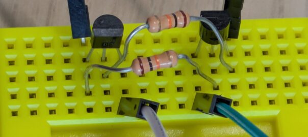
To see this in practice, we can assemble the circuit from basic components. Using a mini-breadboard, I end up with this:

In breadboards, holes are connected along short lines. To make it clearer, I have added red lines to show which holes are connected together, and labelled the components

E stands for Emitter, B for Base and C for Collector. These are the names of transistors pins. The illustration below shows the S8050 NPN transistor pin order and what they correspond to in the schematics. The flat side of the transistor disambiguates the order of the pins.

The circuit behaves exactly like the ESP-Prog, success!

This suggests that our understanding of the ESP-Prog circuit is correct. The fact that this does not behave like we expect from the indicated logic table means that we are missing something else. This is what we will look into in the next article The missing part of Espressif’s reset circuit.

Leave a Reply