- How to use “real” UART
- Arduino’s Automatic Reset
- Linux always toggles DTR & RTS
- Espressif’s Automatic Reset
- Talking to Espressif’s Bootloader
- The ESP32-S2 reset pin
- Reproducing Espressif’s reset circuit
- The missing part of Espressif’s reset circuit
- Transistors in reverse and redundant circuits
- The serial TX path seems to be down
In the previous article, we peeked at the reset circuit of ESP-Prog with an oscilloscope, and reproduced it with basic components. We observed that it did not behave quite as expected. In this article, we’ll look into the missing pieces.


An incomplete circuit
For a hint, we’ll first look a bit more closely at the schematics of the ESP-Prog. Of course, we find the automatic reset circuit itself:

But, right next to it, we find another circuit that can set the electrical level of ESP_EN and ESP_IO0_B:

We can find the physical location of these components in the PDF that describes the PCB layout. Conveniently, you can just hit Ctrl+F and search for SW1/SW2/R7/R8/C16/C19. All of them are situated next to the USB micro-B port:

As indicated by the labels next to the buttons the blue boxes in the schematics SW1 and SW2 correspond to the RST and BOOT press buttons respectively.
We also see two resistors that connect ESP_EN and ESP_IO0_B to the 3.3V rail “VDD3V3”. These are pull-up resistors: when the button is not pressed, they “pull” the electrical level to 3.3V; when the button is pressed, the direct (0Ω) connection to ground “takes priority” over the 10kΩ connection to the 3.3V rail, so the electrical level drops to 0V. In other words, they make it so that the two signals “default” to 3.3V.
There are also two small-value capacitors next to the switches. These are here to debounce button presses. That is, the button momentarily causing multiple contacts due to physical “bouncing”.
However, these components are not actually present in the board. The “(NC)” suffix stands for “Not Connected” and is reaffirmed by the green font. We can verify this visually: if we look closely at each of the locations where R7, R8, C16 and C19 should be, we can see two pads with solder, but no component in between.


These components are not present by default in the board. But users may choose to add them by soldering them manually. This is actually a good hint at what is going on: in some circumstances, we might or might not want to have these components present. And this depends… on the connected board!
The missing pieces
To understand this, we need to look at the schematics of the target board as well. In my case, I will be using ESP32-S2-Saola-1RI. The ESP-Progs’s EN and IO0 pins connect to the Saola’s CHIP_PU (for Power-Up) and GPIO0 pins. We find various circuits connected to these:

The two circuits depicted above are the RST and BOOT buttons of the Saola board. Just like those of the ESP-Prog board, they have an optional capacitor (although of different suggested value) to debounce presses. As long as the button is not pressed, this should not impact the electrical level of CHIP_PU or GPIO0.

Again, the circuit above look very similar to one in the ESP-Prog. This is due to the Saola board having its own UART-to-USB adapter (a CP2102N chip). R28 and R29 are “0Ω resistors”, which means that they act as wires, but can be easily desoldered to disable the automatic reset circuit entirely. However, we are not using the Saola’s UART-to-USB adapter here1.

This is starting to get interesting. We find a 10kΩ resistor R36 that pulls CHIP_PU up to 3.3V and a 1µF capacitor C22 between CHIP_PU and the ground. This time, they are not marked “(NC)”. The schematics of the Saola are slightly less convenient, but we can still locate their physical location by searching the PDF.

From this, we can find them on the board:

This resistor and this capacitor are real! They are not just a figment of our imagination!
There is one final component to find, but we won’t find it in the schematics of the Saola board. We’ll have to take a look at the datasheet of the ESP32-S2 microcontroller itself!


From this, we can deduce that, inside the ESP32-S2 microcontroller, there is a 45kΩ pull-up resistor connected to GPIO0.
Note: I actually assumed a 10kΩ before finding Table 12 and the information below still uses that. However, it should not change anything to the main discussion.
Adding resistors
First, let add the resistors R36 and RPU to the SPICE simulation we used in the previous article.
* Description of the  SS8050 (NPN) transistor
* from https://www.onsemi.com/download/models/lib/ss8050.lib
.MODEL SS8050 NPN
+ IS=3.77207e-13     BF=218.082          NF=1.0409        VAF=32.0909
+ IKF=0.84522        ISE=5.17224e-11     NE=2.12785       BR=5.45795
+ NR=1.06185         VAR=49.0994         IKR=2.19792      ISC=5.17224e-11
+ NC=3.96851         RB=5.74704          IRB=0.1          RBM=0.1
+ RE=0.000841718     RC=0.248242         XTB=0.626944     XTI=1
+ EG=1.05            CJE=2.73346e-11     VJE=0.721406     MJE=0.85
+ TF=6.43938e-10     XTF=1.43228         VTF=0.344801     ITF=1.20072
+ CJC=2.60002e-11    VJC=0.4             MJC=0.367851     XCJC=0.1
+ FC=0.9999          CJS=0               VJS=0.75         MJS=0.5
+ TR=1e-07           PTF=0               KF=0             AF=1

* 3.3 V rail
VCC  VCC  0   3.3

* Input pattern
VDTR DTR 0   PWL(0ms 3.3 4ms 3.3 4ms 0 6ms 0 6ms 3.3 16ms 3.3 16ms 0 18ms 0 18ms 3.3)
VRTS RTS 0   PWL(0ms 3.3 8ms 3.3 8ms 0 10ms 0 10ms 3.3 12ms 3.3 12ms 0 14ms 0 14ms 3.3 16ms 3.3 16ms 0 18ms 0 18ms 3.3)

* NPN transistors (collector, base, emitter)
Q1  EN  B1 RTS  SS8050
Q2  IO0 B2 DTR  SS8050

* Resistors on bases of the transistors
R21 DTR B1  10k
R22 RTS B2  10k

* Pull-up resistors on the collectors of the transistors
RPU1 EN  VCC 10k
RPU2 IO0 VCC 10k

* Simulation
.tran 10u 24m 0 10n
This is the result:

This is promising! Although there are a few artifacts (which could just be inaccuracies of the simulation), EN and IO0 are behaving as we expect!
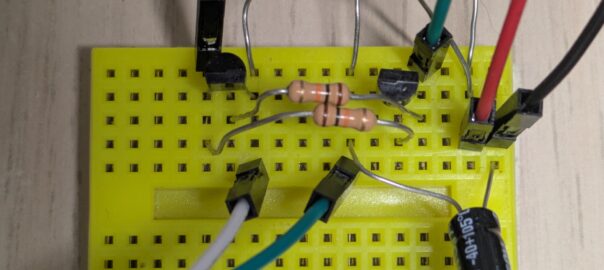
We can also add these resistors to the breadboard circuit:

When I run the same C program as before and observe the behavior on an oscilloscope, this is what I observe:
This is exactly the behavior we expected from the logical gate! We are done!
But… are we?
Connecting a board
Let’s connect the ESP-Prog to the Saola board, and see how it behaves in a realistic situation.

This is still slightly different from what we expect. For a quick sanity check, let’s see how the basic breadboard circuit (without the pull-ups) behaves if we connect it to the Saola board.

This is virtually identical. We can zoom in on EN and IO0 to confirm:


What we are seeing is the capacitor slightly delaying the rise of EN, relative to the rise of IO0 to avoid any ambiguity.
If we wanted to restart the board into bootloader mode, we would first toggle RTS (bringing it low), causing EN to also become electrically low, and turning the microcontroller off. We would then flip both DTR and RTS, bringing them electrically low and high, respectively; this would result in:
- EN becoming electrically high, thus starting the microcontroller
- IO0 becoming electrically low, which the microcontroller would interpret as a choice to start in bootloader mode
However, without the capacitor, the microcontroller could measure IO0 before it actually rose to 3.3V thus failing to select bootloader mode. With it, IO0 will rise to 3.3V even before EN could start the chip. You can see this in the screenshot below.

This is actually documented in page 18 of the ESP32-S2 datasheet:

The minimum value given for tSU is 0 ms, but that does not mean that things will work without the capacitor. Multiple people had issues related to a missing delay: [1], [2], [3]. See also another investigation of the reset circuit here.
So, let’s add C22, the capacitor we found in the Saola’s schematics!
Adding a capacitor
First, in the SPICE simulation:
* Description of the  SS8050 (NPN) transistor
* from https://www.onsemi.com/download/models/lib/ss8050.lib
.MODEL SS8050 NPN
+ IS=3.77207e-13     BF=218.082          NF=1.0409        VAF=32.0909
+ IKF=0.84522        ISE=5.17224e-11     NE=2.12785       BR=5.45795
+ NR=1.06185         VAR=49.0994         IKR=2.19792      ISC=5.17224e-11
+ NC=3.96851         RB=5.74704          IRB=0.1          RBM=0.1
+ RE=0.000841718     RC=0.248242         XTB=0.626944     XTI=1
+ EG=1.05            CJE=2.73346e-11     VJE=0.721406     MJE=0.85
+ TF=6.43938e-10     XTF=1.43228         VTF=0.344801     ITF=1.20072
+ CJC=2.60002e-11    VJC=0.4             MJC=0.367851     XCJC=0.1
+ FC=0.9999          CJS=0               VJS=0.75         MJS=0.5
+ TR=1e-07           PTF=0               KF=0             AF=1

* 3.3 V rail
VCC  VCC  0   3.3

* Input pattern
VDTR DTR 0   PWL(0ms 3.3 4ms 3.3 4ms 0 6ms 0 6ms 3.3 16ms 3.3 16ms 0 18ms 0 18ms 3.3)
VRTS RTS 0   PWL(0ms 3.3 8ms 3.3 8ms 0 10ms 0 10ms 3.3 12ms 3.3 12ms 0 14ms 0 14ms 3.3 16ms 3.3 16ms 0 18ms 0 18ms 3.3)

* NPN transistors (collector, base, emitter)
Q1  EN  B1 RTS  SS8050
Q2  IO0 B2 DTR  SS8050

* Resistors on bases of the transistors
R21 DTR B1  10k
R22 RTS B2  10k

* Pull-up resistors on the collectors of the transistors
RPU1 EN  VCC 10k
RPU2 IO0 VCC 10k

* Capacitor between EN and ground
C22 EN GND 1uF

* Simulation
.tran 10u 24m 0 10n

On EN, we see something very close to what we expect, with a slow rise, instead of a sharp edge.

We can again measure the breadboard circuit on its own (no Saola board connected to it):

EN now behaves almost exactly as the ESP-Prog connected to the Saola board. The slight difference in the shape of the rising slop on EN will be discussed in the next article. As far as I can tell, the slight voltage drops on IO0 are due to the behavior of the ESP32-S2 chip itself when it is powered down.

Wrapping up
From these experiments, we have gained a pretty solid grasp of the circuit used for automatically resetting the microcontroller into bootloader mode in Espressif boards. You can play with the simulation below to see it in action. The most interesting sequence of action is the one used to trigger the reset into bootloader mode:
- Toggle the switch next to RTS to make it electrically low.
- Pause the simulation by clicking on the “RUN / Stop” button in the upper right.
- Toggle the switch next to DTR to make it electrically low.
- Toggle the switch next to RTS to make it electrically high.
- Resume the simulation by clicking on the “RUN / Stop” button in the upper right.
- Wait and observe the electrical levels of EN and IO0.
Addendum
The C program below shows what Espressif’s programmer tool will typically do when opening the serial device, restart the target board normally, or restarting it in booloader mode.
#define _XOPEN_SOURCE 500 // needed for usleep()
#include <stdio.h> // puts()
#include <fcntl.h> // open(), O_RDWR, O_NOCTTY
#include <unistd.h> // usleep()
#include <sys/ioctl.h> // ioctl(), TIOCMSET, TIOCM_RTS, TIOCM_DTR
#include <stdlib.h> // exit()

void tiocmset(int fd, int mask) {
    if (ioctl(fd, TIOCMSET, &mask) < 0) {
        puts("Failed to set mode");
        exit(1);
    }
    usleep(100000); // 100ms
}

int main(void) {
    int fd = open("/dev/ttyUSB1", O_RDWR | O_NOCTTY);
    if (fd < 0) {
        puts("Failed to open device");
        return 1;
    }
    sleep(1);

    while (1) {

        // Use ONE of these three blocks

        // OPENING SERIAL DEVICE
        // assert both DTR and RTS = no effect
        tiocmset(fd, TIOCM_DTR | TIOCM_RTS);
        // clear = no effect
        tiocmset(fd, 0);

        // NORMAL RESTART
        // assert RTS = turn off
        tiocmset(fd, TIOCM_RTS);
        // clear = start normally
        tiocmset(fd, 0);

        // REBOOT IN BOOTLOADER MODE
        // assert RTS = turn off
        tiocmset(fd, TIOCM_RTS);
        // assert DTR and clear RTS = start into bootloader mode
        tiocmset(fd, TIOCM_DTR);
        // clear = no effect
        tiocmset(fd, 0);

        sleep(1);
    }
}
The screenshots below show the measurements with my oscilloscope for each case, using the ESP-Prog with the Saola board, or the breadboard circuit.


- I realized later that this approximation was not correct, as explained in the next article. ↩︎

Leave a Reply