The previous series of articles about UART was initially motivated by an error I was getting when using the ESP-Prog. I could have jumped straight to the conclusion, but I took the time to really understand what was going on, and we are finally reaching the end of this investigation.
- How to use “real” UART
- Arduino’s Automatic Reset
- Linux always toggles DTR & RTS
- Espressif’s Automatic Reset
- Talking to Espressif’s Bootloader
- The ESP32-S2 reset pin
- Reproducing Espressif’s reset circuit
- The missing part of Espressif’s reset circuit
- Transistors in reverse and redundant circuits
- The serial TX path seems to be down
Connecting to “real” UART again
I already used the ESP-Prog in previous articles, but this part was written before any of them, so it goes back to some fundamentals.
The main change from the first article is that we will be using the ESP-Prog (~13 € on AliExpress) instead of any generic UART-to-USB programmer. It provides two interfaces, each of which with a small (1.77mm pitch) and large (2.54mm pitch) connectors:
- “Program”, to send a program to the target microcontroller. This is actually mostly just UART.
- “JTAG”, which is a more complex protocol for debugging programs while they run on microcontrollers, but we are not interested in that today.

The connectors are designed for a custom cable that you plug in the small connector. As far as I can tell, the only Espressif devkits that use it are:
All these are marked as “end of life”. All other devkits include a UART-to-USB bridge (i.e. an additional chip) that exposes the UART port of the microcontroller over USB. This is convenient since the devkits use USB for power anyway, but it makes it harder to understand the interaction with the microcontroller.
In any case, we will not use the provided cable and directly plug jumper wires in the large connector. The pinout (which pins to use for what) is provided in the documentation of the ESP-Prog, but labels are also printed right next to the pins:

However, note that there is a catch. Here, TXD0 on the ESP-Prog should be connected to the TX pin of the target board (not RX), and RXD0 should be connected to RX (not TX). The naming is a convention, so try not to think too deep about it.

With everything properly connected, you should be able to reproduce the small experiment from the previous tutorial.
Note: The ESP-Prog exposes two USB devices: one for JTAG, one for UART. As indicated, JTAG will show up as “COM n” (e.g. COM1) and UART as “COM n+1” (e.g. COM2) on Windows. On Linux, that would give you /dev/ttyUSB0 for JTAG and /dev/ttyUSB1 for UART1, assuming no other UART device is connected. You will want to use /dev/ttyUSB1.

The serial TX path seems to be down
Now, the entire purpose of Talking to Espressif’s Bootloader was to give us some way to test the talking to the chip over UART. In other words, we will need to:
- Run
esptool --baud=115200 --chip=esp32s2 --port=/dev/ttyUSB0 flash_id - Reset the chip in bootloader mode
In The missing part of Espressif’s reset circuit, we learned that the reset mechanism of the ESP-Prog could not be used reliably to control the Saola board. Instead, we’ll be doing it manually, with the following sequence of actions:
- Press and hold the “BOOT” button on the Saola board
- Press and release the “RST” button on the Saola board
- Release the “BOOT” button on the Saola board
If we do this while the esptool command is running, we get:
% esptool --chip=esp32s2 --port=/dev/ttyUSB1 flash_id
esptool.py v4.7.0
Serial port /dev/ttyUSB1
Connecting......................................

A fatal error occurred: Failed to connect to ESP32-S2: Download mode successfully detected, but getting no sync reply: The serial TX path seems to be down.
For troubleshooting steps visit: https://docs.espressif.com/projects/esptool/en/latest/troubleshooting.html
In other words, the program was able to receive the boot message (see below) from the Saola board, but nothing seems to have happened when it sent commands to it, indicating that data is being transmitted from the board to the computer, but not the other way around.
ESP-ROM:esp32s2-rc4-20191025
Build:Oct 25 2019
rst:0x1 (POWERON),boot:0x0 (DOWNLOAD(USB/UART0/1/SPI))
waiting for download
If you have followed the previous articles on this blog, the reason might now be obvious: the UART-to-USB adapter in the Saola board interferes with the one in the ESP-Prog!
Indeed, even if we do not connect a USB cable into the Saola board, its UART-to-USB adapter turns on and tries to control the UART lines. In the previous articles, it caused the reset circuitry to not work correctly. To understand while it only impedes the “TX path”, but not the “RX path”, let’s look at each in detail.

For the purpose of clarity, I have numbered the various TX/RX pins:
- TX1/RX1 for the ESP32-S2
- TX2/RX2 for the CP2102N, which is the UART-to-USB adapter on the Saola board
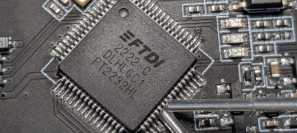
- TX3/RX3 for the FT2232HL, which is the UART-to-USB adapter on the ESP-Prog
RX path. When the ESP32-S2 microcontroller sends data, it sets its TX1 pin electrically high or low as needed. This is connected both to:
- the RX2 pin of CP2102N; the chip reads the electrical levels and would transmit the signal if it were connected with USB;
- the RX3 pin of the FT2232HL; the chip reads the electrical levels and transmits the signal through the USB cable.
In other words, the electrical level is set only by the ESP32-S2, and successfully read by both UART-to-USB adapter chips. The esptool can successfully receive data transmitted by the ESP32-S2 microcontroller.
TX path. In the other direction, the ESP32-S2 receives data on its RX1 pin. This is connected to:
- the TX2 pin of the CP2102; although no USB cable is connected, the chip is still active, and sets the electrical signal to high,
- the TX3 pin of the FT2232HL; when it receives data from the USB cable, its sets the electrical signal to high or low.
In other words, the CP2102 and FT2232HL “fight” to set the electrical level of RX1. If the CP2102 “wins”, the ESP32-S2 receives no data. Thus, “The serial TX path seems to be down”.
Under the oscilloscope
We can see this in action by connecting an oscilloscope to observe the electrical levels of TX1 and RX1. The simplest way to achieve this is to attach the probes to the wires between TXD0 and between RXD0.
If the Saola board is running with its usual firmware and we do nothing in particular, this is what we observe:

red... goes through the RX path
green... goes through the RX path
blue... goes through the RX pathThese are the periodic messages sent by the ESP32-S2 while it changes the color of its RGB LED. Considering that each vertical gradation corresponds to 2V, we can see that the electrical signal varies between 0 V and something close to 3.3 V, as expected.
If we reset the board while looking at the UART signals, we can also see the boot sequence:

ESP-ROM:esp32s2-rc4-20191025Now, what happens if we run esptool?

We can see a message being sent through the TX path. It looks meaningless, but this is actually successfully decoded by the oscilloscope. This is indeed part of the “synchronization sequence”:
  c000082400000000 0007071220555555 | ...$........ UUU
  5555555555555555 5555555555555555 | UUUUUUUUUUUUUUUU
  5555555555555555 5555555555c0     | UUUUUUUUUUUUU.
However, the electrical level does not vary between 0 V and 3.3 V. It seems to drop only to around 2V, not even half-way through. Here, we are observing the CP2102 trying to set the electrical level high. The ESP32-S2 probably expects the electrical level to drop by at least half and, as a result, it does not see the transmitted signal.
Mystery solved! Now, how do we fix it?
Desoldering 0Ω resistors
Now, we have two chips competing to set the electrical level. We want to use the FT2232RL and the CP2102N is just squashing our hopes and dreams. The solution, of course, is just to cut it out.
In fact, Espressif’s engineers have already thought about this case, and provided a simple way to achieve this:

On the Saola board, the pins TXD and RXD of the CP2102N are connected respectively to U0RXD and U0TXD through 0Ω resistors, R34 and R35. Since their value is 0Ω, they don’t serve as actual resistors. Their purpose is to be optionally desoldered. And this is exactly what I did!

We can run the same experiment with the modified board to make sure this actually solves our problem.

esptool through an ESP-Prog connected to the modified Saola board.It works! The electrical signal drops to 0 V, as expected, and esptool successfully completes:
$ esptool --chip=esp32s2 --port=/dev/ttyUSB1 flash_id
2025-08-11 22:06:01.77+0200
esptool.py v4.7.0
Serial port /dev/ttyUSB1
Connecting....
Chip is ESP32-S2 (revision v0.0)
Features: WiFi, No Embedded Flash, No Embedded PSRAM, ADC and temperature sensor calibration in BLK2 of efuse V2
Crystal is 40MHz
MAC: 68:67:25:2d:f6:a2
Uploading stub...
Running stub...
Stub running...
Manufacturer: 5e
Device: 4016
Detected flash size: 4MB
Flash type set in eFuse: quad (4 data lines)
Hard resetting via RTS pin...
Current drive
For a last segue, I noticed that I only encountered the problem when using the ESP-Prog. When connecting to the unmodified Saola board using my FT232RL adapter, or even my CH340G one, everything worked fine. This is confirmed by looking at the oscilloscope.

esptool through an FT232RL UART-to-USB adapter with an unmodified Saola boardYou might notice that the electrical level does not quite go to 0 V, but it is still much lower than when using the ESP-Prog. To understand this, I needed to find the amount of current that each of the CP2102N (Saola board), the FT2232H (ESP-Prog) and FT232RL (UART adapter) can supply. Unfortunately, the information is not easy to get from their datasheets. However, while reading that of the FT2232H, I noticed something intriguing:
“Configurable I/O drive strength (4, 8, 12 or 16
mA) and slew rate.” (source)
Unlike the CP2102N and the FT232RL, you can actually select the maximum current that the FT2232H provides (to set the electrical level high) or sinks (to set the electrical level low). For this, you need to download the FT_PROG utility from FTDI. When connected through USB to the ESP-Prog, it lets us change various parameters of the FT2232H:

In the ESP-Prog, TX and RX correspond to the pins BDBUS0 and BDBUS1 of the FT2232H (see below).

AD/AC/BD/BC does not map neatly to AL/AH/BL/BH, so I was not sure which one I should change. In doubt, I changed them all:

By setting the drive current to the maximum value of 16 mA, I was able to use the ESP-Prog with the unmodified Saola board, just like with the FT232RL adapter!

esptool through the ESP-Prog after setting drive current to 16 mA with an unmodified Saola boardAnyway, this is just a nice-to-know. This results in up to 16 mA being needlessly provided by the CP2102N and sunk by the FT2232H. The proper way to fix this is still to remove the 0Ω resistors.